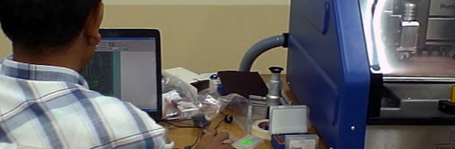
Printed Circuit Laboratory
The PCB (Printed Circuit Board) laboratory is intended to fabricate prototype PCB boards of various kinds for experimental, educational and professional purposes. The fabrication procedure is based on computer controlled mechanical drilling and milling of copper coated circuit boards. Chemical and other methods are not used. The completion of a single PCB takes a considerable time and therefore the equipment cannot be used for fabriactions of bulk amounts.
The laboratory is equipped with a very sensitive (.25 µm resolution) milling and drilling machine connected to a computer with related CAD/CAM software installed, a working stand with an integrated camera and monitor system for placement operations of SMD (surface mounted device) components and a reflow (lead-free) oven to fix electronic circuit components onto the board for a complete fabrication of PCB prototype. The laboratory is also capable of fabricating RF boards.
The laboratory is primarly intended for researchers and senior students of the department. Also, our beginner students who work with PCB design are supported partially by this laboratory. Seminar sessions are being held from time to time to make students familiar with PCB design and fabrication procedures.
As a standard, Gerber-X fabrication output file format is accepted and used in the laboratory projects.
Important Points to Pay Attention During the Design Phase
There are some prerequisites and limitations to take into consideration prior to the fabrication as the materials used have some certain physical properties:
- Milling Constrains:
- At least 0.15 mm of track witdh
- At least 0.15 mm of isolation between tracks
- At least 0.15 mm of drill hole diameter
- Maximum of 305x229 mm2 (12"x9") working plate size
- Constraints if Masking is Required:
- At least 0.4 mm of pad's narrowest edge
- Minimum of 0.5 mm of isolation between pads
- Constraints if Component Placement is Required:
- At least 0.2 mm of pad's narrowest edge for SMDs
- Minimum of 0.4 mm of isolation between pads
- Besides, the constraints mentioned in the item-b above should be noted as a masking operation would be useful or necessary during the placement step.
Technical information about maximum temperature values that the circuit components can withstand must also be taken into consideration prior to the reflow step.
Note that the technical values mentioned above may change within certain tolerance limits in some particular cases.
Laboratory Working Principles
The owner of the project must supply
- Gerber files necessary for fabrication such as Top Layer, Bottom Layer, Board Outline, Drill Plated / Unplated and Aperture Tool Lists;
- All the circuit components to be used on the prototype PCBs and sufficient amount of lead-free solder that is suitable for that specific prototype;
- Plain copper boards if their particular properties (such as dielectric constants, depth of boards, etc.) are vital for the project to work correctly.
The owner of the project should contact the laboratory personnel and get an appointment beforehand. At the time of appointment, he/she must submit the Gerber output files to the laboratory personnel. The delivery date of the final product, then, will be fixed after the personnel and the project's owner discuss and agree on the technical details.
Please note that the laboratory has currently no capabilites to make through-hole plating, labelling and multilayer PCB fabrication.